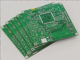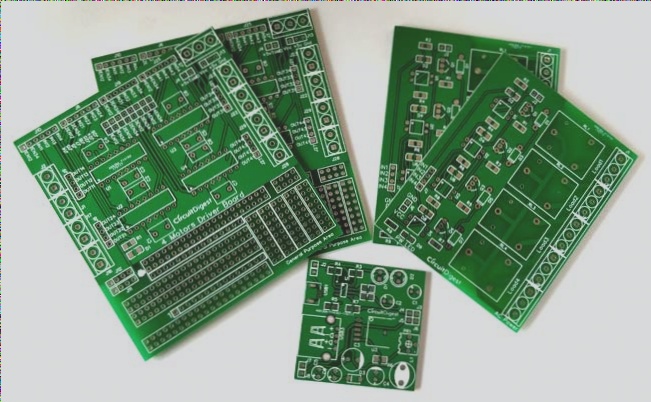
Methods and Techniques for Controlling the PCB Etching Process
The PCB manufacturing process involves complex physical and chemical reactions to form circuit patterns from a light board. This article focuses on the final crucial step: etching, using the predominant “pattern plating method” where copper foil is selectively dissolved after applying a lead-tin resist layer. Alternative methods include using photosensitive film or a full board copper plating process, each impacting production complexity and quality.
Methods and Techniques for Controlling the PCB Etching Process Read More »