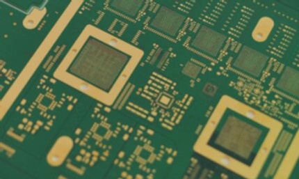
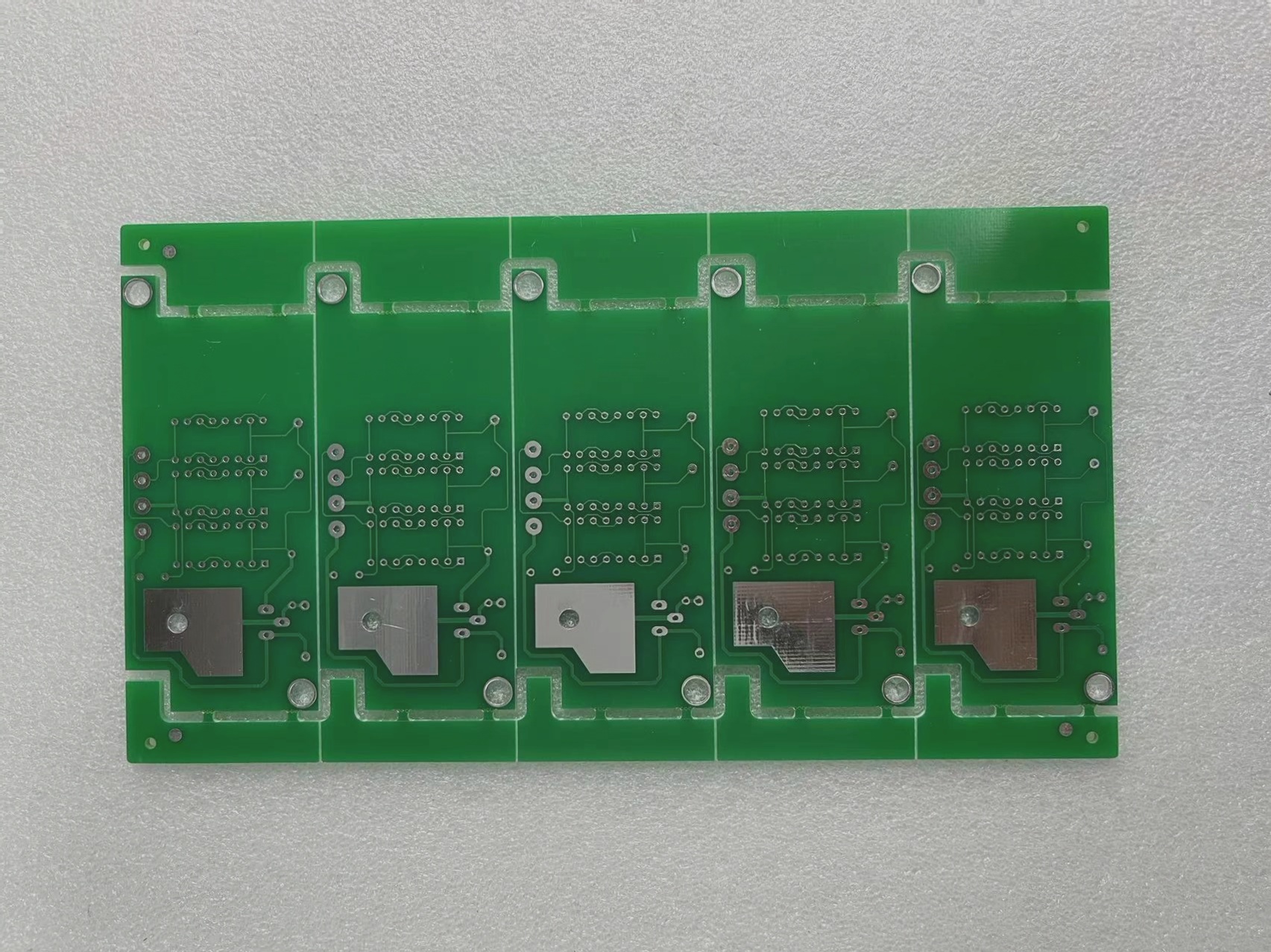
1. 20-layer PCB is widely used in consumer electronics, communication electronics, computers, automation, medical devices, defense, aerospace and military applications. Its manufacturing process involves imaging, etching, pressing, processing and copper plating. The design specifications require high-speed and high-capacity operation, heat resistance, and 20 alternating layers of copper substrate. The advantages include high assembly density, small volume, light weight, reduced wiring, simple installation, high reliability, increased design flexibility and the ability to form circuits with certain impedance. Due to its flexible design, stable electrical performance and superior economic performance, 20-layer PCB has been widely used in the production of electronic products.


