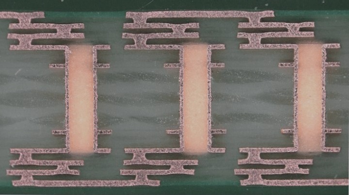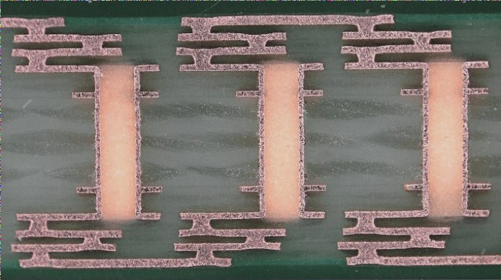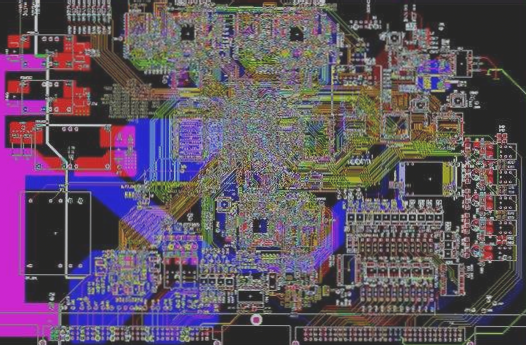
Via design expertise in PCB (Printed Circuit Board) layout and design.
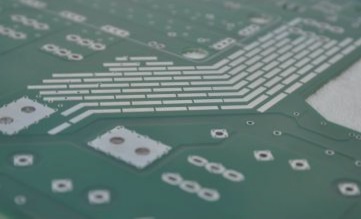
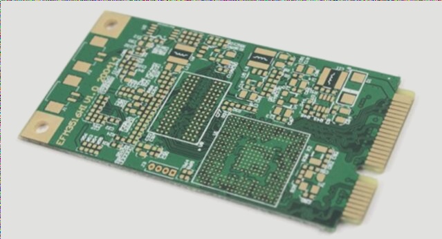
In PCB design, vias are essential for layer-to-layer connections and component positioning, with types including **blind**, **buried**, and **through** vias, each affecting manufacturing cost, performance, and design complexity, with through vias being the most commonly used due to their cost-effectiveness and ease of integration.
Via design expertise in PCB (Printed Circuit Board) layout and design. Read More »