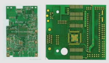
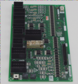
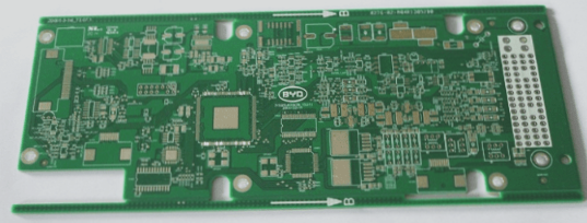
circuit board layout

PCB Materials and Strategic Component Placement

A printed circuit board (PCB) consists of various elements like pads, vias, traces, and components, each serving specific functions, and its layout must consider factors such as component placement, size, signal integrity, heat dissipation, and manufacturing cost to ensure functionality, performance, and reliability.

PCB Materials and Strategic Component Placement Read More »

Emphasize the evaluation of the PCB design workflow.

After finalizing a PCB layout and routing, a critical yet often overlooked step is post-inspection, which is essential to prevent issues like insufficient trace width and improper component placement that could lead to costly manufacturing problems.

Emphasize the evaluation of the PCB design workflow. Read More »

How to design the PCB for a single-chip control board?

The circuit board design process involves three main steps: circuit schematic design, netlist generation, and PCB design, emphasizing careful component placement, decoupling capacitor positioning, and effective ground wire design to minimize interference and enhance reliability.

How to design the PCB for a single-chip control board? Read More »

Grid Configuration Techniques and Quality Control in PCB Layout Design

In PCB design, components should be placed on the same side for optimal layout, with a minimum distance of 1 mm between adjacent components and at least 2 mm from the board edge, while ensuring a compact, uniform, and functional arrangement; quality control in PCB proofing involves rigorous checks and independent testing to address potential issues before mass production.

Grid Configuration Techniques and Quality Control in PCB Layout Design Read More »

Contact

WellCircuits
More than PCB

Upload your GerberFile(7z,rar,zip)