circuit design

Techniques and Characteristics of PCB Duplication and Drilling

PCB copying techniques involve reverse engineering, including steps like board reading, component removal, schematic reconstruction, and layout adaptation, to replicate electronic designs, with a focus on precision and the use of advanced tools for testing and micro-hole drilling.

Techniques and Characteristics of PCB Duplication and Drilling Read More »

Reflection resulting from variations in PCB trace width

When PCB trace widths change, impedance variations can cause signal reflections, which may be significant depending on the impedance change magnitude, signal rise time, and trace length; careful analysis and impedance matching can mitigate these effects.

Reflection resulting from variations in PCB trace width Read More »

Guidelines for Utilizing a PCB Prototype Board

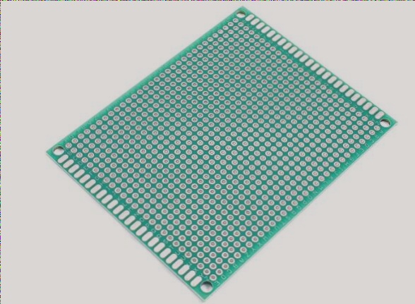
PCB prototype boards facilitate rapid and flexible circuit development through component insertion, soldering on pre-drilled pads, and integration into prototype PCBA boards, ensuring efficient testing and validation of electronic designs.

Guidelines for Utilizing a PCB Prototype Board Read More »

Guide to High-Speed Printed Circuit Board Routing Practices

Effective PCB wiring is crucial for high-speed circuits, beginning with a meticulously crafted schematic that guides signal flow. Comprehensive schematics are invaluable for resolving circuit issues, requiring detailed inclusion of waveform diagrams, mechanical details, component placements, and impedance controls to ensure premium quality and optimal performance.” Let me know if there’s anything else you need!

Guide to High-Speed Printed Circuit Board Routing Practices Read More »

Copper peel-off on PCB: causes and solutions.

Copper foil over-etching in PCB fabrication can be caused by changes in specifications without adjusting etching parameters, poor drying after etching, local collisions during the PCB process, and unreasonable circuit design. This can result in excessive corrosion, separation of the zinc layer, and copper wire fall-off.

Copper peel-off on PCB: causes and solutions. Read More »

PCB ESD Overview: In-depth Analysis

Effective ESD protection is paramount in electronic product design, mitigating risks of product crashes or component damage caused by static electricity through methods like avalanche diode clamping, capacitors, ferroxide beads, tip discharge, LC filters, multilayer boards, and isolation-based protection.

PCB ESD Overview: In-depth Analysis Read More »

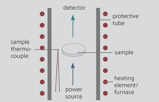
Intro to Laser Flash Analysis & Design in PCBA Manufacturing”

Understanding the importance of adept thermal management in PCB design and manufacturing, including the role of laser flash analysis in determining thermal diffusivity, is crucial for ensuring optimal performance and reliability.

Intro to Laser Flash Analysis & Design in PCBA Manufacturing” Read More »

Factors Leading to Detachment of Copper Traces on Impedance-Controlled

Copper wire detachment on impedance circuit boards can be attributed to issues such as over-etched copper foil, residual etching solution, unreasonable circuit design, abnormal electrolytic copper foil, and poor etching of potion. Selecting a manufacturer with robust process capabilities and quality materials can help mitigate this problem.

Factors Leading to Detachment of Copper Traces on Impedance-Controlled Read More »

Common Defects and Specifications of Chip Capacitors

1. The main manifestations of chip capacitor failure include various issues encountered during SMD capacitor maintenance. 2. Parameters crucial for selecting chip capacitors in circuit design encompass factors essential for their suitability in a given circuit.

Common Defects and Specifications of Chip Capacitors Read More »

Contact

WellCircuits
More than PCB

Upload your GerberFile(7z,rar,zip)