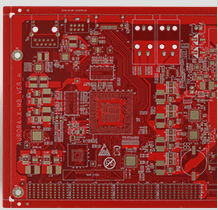
circuit routing

What is reverse engineering of PCB schematics?

In PCB reverse engineering, the process involves creating a schematic diagram from the physical PCB or documentation, which is then used to analyze functional characteristics, divide the design into functional areas, select reference components, and correctly route traces, followed by optimization and validation to ensure accuracy and clarity.

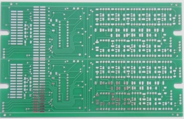
What is reverse engineering of PCB schematics? Read More »

How to optimize the PCB power supply layout to minimize EMI

A well-designed power supply PCB layout is crucial for circuit performance, with attention to component positioning, EMI filtering, and minimizing noise coupling to optimize efficiency and reduce revisions during product development.

How to optimize the PCB power supply layout to minimize EMI Read More »

Contact

WellCircuits
More than PCB

Upload your GerberFile(7z,rar,zip)