Grid Configuration Techniques and Quality Control in PCB Layout Design
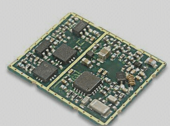
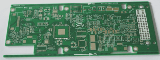
In PCB design, components should be placed on the same side for optimal layout, with a minimum distance of 1 mm between adjacent components and at least 2 mm from the board edge, while ensuring a compact, uniform, and functional arrangement; quality control in PCB proofing involves rigorous checks and independent testing to address potential issues before mass production.
Grid Configuration Techniques and Quality Control in PCB Layout Design Read More »