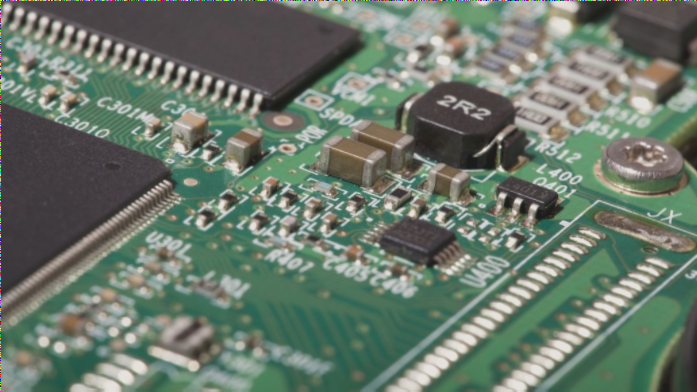
Comprehensive PCB Design Process
The process of designing a PCB schematic involves searching for existing components in the library or creating new ones if necessary, ensuring proper component pin configurations, running component rule checks, and following a structured workflow for accuracy and compliance with electrical standards.