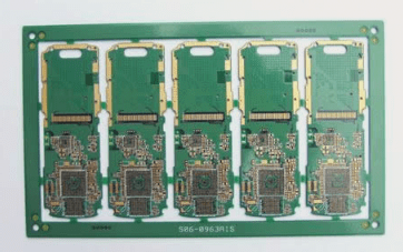
Introduction to Silk Screening on Multi-Layer PCB Boards
**PCB Screen Printing Specifications and Requirements**: Ensure all components, holes, and orientation marks are clearly labeled on the silk screen, avoid screen coverage on pads and vias, and include necessary information like board name, date, and barcode for easy identification and functionality.
Introduction to Silk Screening on Multi-Layer PCB Boards Read More »

