Collection of Knowledge on PCB Copper Content
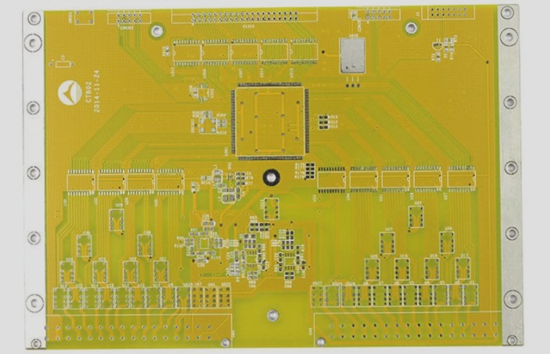
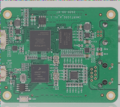
Copper pour is a PCB technique where unused areas are filled with copper to improve signal integrity, reduce interference, lower impedance, and enhance power efficiency, with considerations for ground connections, safety spacing, and routing rules to avoid errors.