Copper electroplating

Layer thickness of 6-layer PCB

A 6-layer PCB, also known as a “multi-layer board,” consists of three copper-clad laminates, undergoing cutting and sequential pressing of inner layers with drilled holes, followed by subsequent pressing, drilling, copper electroplating, and is commonly utilized in the communications industry.

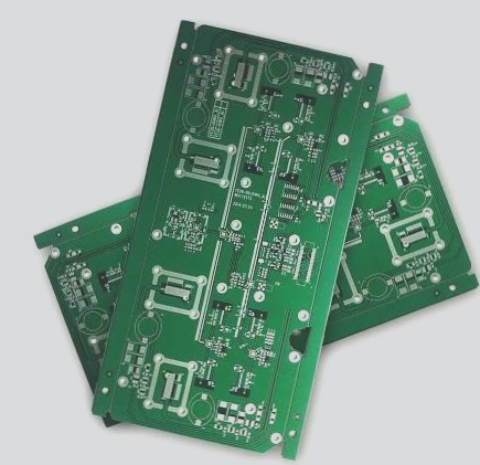
Layer thickness of 6-layer PCB Read More »

Concise Analysis of Copper Electroplating Process in PCB Manufacturing

The PCB board electroplating process includes acid bright copper electroplating, nickel/gold electroplating, and tin plating, with processes such as pickling, full board copper plating, pattern transfer, acid degreasing, micro-etching, and pattern copper plating to ensure uniform thickness distribution and bonding for optimal functionality.

Concise Analysis of Copper Electroplating Process in PCB Manufacturing Read More »

Common Issues and Remedies in the PCB Copper Sulfate Electroplating Process 1

Copper electroplating is essential for improving coating adhesion and corrosion resistance, particularly in the PCB process. Common problems such as rough electroplating can be solved by reducing the current and checking for abnormalities.

Common Issues and Remedies in the PCB Copper Sulfate Electroplating Process 1 Read More »

Contact

WellCircuits
More than PCB

Upload your GerberFile(7z,rar,zip)