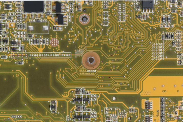
copper filled vias

Principles for Layer Selection and Stacking in PCB Design

Before designing a multi-layer PCB, it’s crucial to determine the board structure based on circuit scale, size, and EMC needs, choose the number of layers, and optimize the laminated structure for routing efficiency and electromagnetic interference suppression while considering manufacturing constraints.

Principles for Layer Selection and Stacking in PCB Design Read More »

Design and development of PCBs for robot controllers

Research focuses on designing and developing mobile PCB controllers for micro-probing robots, emphasizing task-specific surveillance capabilities in diverse environments, due to current limitations in fully autonomous operation and communication reliability.

Design and development of PCBs for robot controllers Read More »

Comprehend the design principles of PCBA boards

The PCB design process involves three main steps: schematic design, netlist generation, and PCB layout. Specific requirements include optimizing component placement and trace routing to minimize interference, such as separating parallel signal lines with a ground wire and aligning adjacent layer traces perpendicularly. Effective grounding involves placing separate power and ground planes perpendicular across layers. Trace widths are critical, with wider ground traces recommended for digital circuit PCBs to establish a robust ground network.

Comprehend the design principles of PCBA boards Read More »

The positioning device requires an urgent PCB upgrade.

Domestic positioning devices face a technological gap compared to international counterparts, and utilizing PCB copy boards for reverse engineering and upgrading can help bridge this gap and advance core technology and accuracy in positioning systems.

The positioning device requires an urgent PCB upgrade. Read More »

Strategies for Preserving Value in Four-Layer PCBs

The revised text covers: 1. IPC standard-defined quality of four-layer PCBs with anti-oxidation treatment and storage guidelines; 2. The structure and layer usage of a four-layer PCB, emphasizing the importance of proper layer management and routing techniques; 3. Design principles for multi-layer PCBs, including spacing of traces, line cornering options, trace width determination, and strategies for reducing interference.

Strategies for Preserving Value in Four-Layer PCBs Read More »

Control Method for Etching Process in PCB Fabrication

PCB etching methods vary, including pattern electroplating and full board copper plating, each influencing quality and efficiency, with issues like side corrosion impacting process uniformity.

Control Method for Etching Process in PCB Fabrication Read More »

Outline Anti-ESD Strategies in PCB Design

In PCB design, enhance anti-ESD capabilities through layered construction, optimized layout, and meticulous installation, focusing on minimizing impedance and inductive coupling. Employ multilayer PCBs with ground and power planes, tightly interlaced power and ground grids for double-sided boards, and compact, centrally located circuits. Incorporate extensive chassis grounding, maintain isolation zones, and use protective components strategically to achieve effective ESD prevention.

Outline Anti-ESD Strategies in PCB Design Read More »

PCB Design Considerations and the Impact of PCB Damage on Electronic Components

When making PCB circuit boards, consider substrate choice, production environment, technological processes, and the handling of damage to electronic components like resistors, capacitors, and integrated circuits to ensure optimal performance and reliability.

PCB Design Considerations and the Impact of PCB Damage on Electronic Components Read More »

Contact

WellCircuits
More than PCB

Upload your GerberFile(7z,rar,zip)