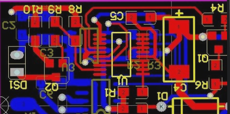
Principles of PCB Anti-Jamming Design
The guidelines for PCB power line layout emphasize optimizing power and ground trace width, proper decoupling capacitor placement, and careful separation of digital and analog grounds, while minimizing interference through proper component positioning, trace routing, and shielding techniques.


