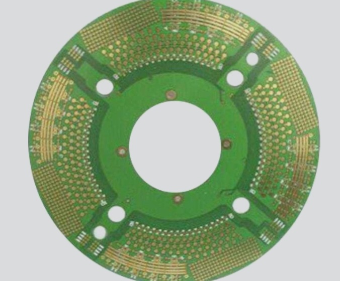
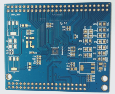
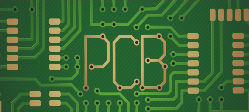
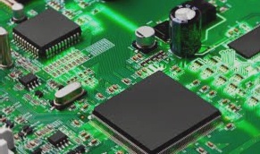
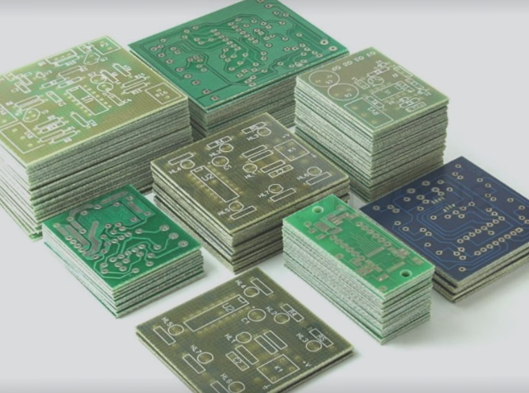
double-sided PCB

How are double-sided printed circuit boards (PCBs) manufactured?

The double-sided PCB manufacturing process includes methods like SMOBC (Solder Mask Over Bare Copper) and pattern plating, with key steps such as electroless copper plating, lead-tin stripping, hole plugging, and hot air leveling, aimed at improving solderability, reliability, and circuit integrity.

How are double-sided printed circuit boards (PCBs) manufactured? Read More »

How can one ascertain the number of layers required for a PCB design?

To determine the number of layers in a PCB, observe the via holes and light transmission: if vias are visible on both sides, it’s likely a 4-layer board; if vias are visible only on one side or light passes through them, it could be a 6/8-layer board; multilayer boards with opaque inner cores may have many more layers.

How can one ascertain the number of layers required for a PCB design? Read More »

Guidelines for Copper Trace Routing on Printed Circuit Boards

This text discusses various aspects of circuit board design, including current density considerations, the use of design software, the advantages of double-sided and multi-layer boards for reliability and routing, and guidelines for pad sizing, component attachment, and effective wiring to ensure optimal performance and thermal management in electronic applications.

Guidelines for Copper Trace Routing on Printed Circuit Boards Read More »

Layout, signal integrity, or thermal management

Single-sided printed circuit boards are cost-effective and commonly used in consumer electronics, while double-sided and multilayer boards are employed for more complex interconnections and higher reliability, with flexible circuits and metal cores used for specific needs, all designed according to standardized grids and production conditions.

Layout, signal integrity, or thermal management Read More »

Fundamentals of PCB Board Lamination Process

The development of modern electronic science and technology increasingly demands higher precision in PCBs, with lamination playing a pivotal role in embedding copper layers within substrates to prevent unintended signal conduction or current flow. Various laminating processes cater to different PCB types, including multilayer and double-sided boards, as well as specialized laminates like PTFE for RF applications. PCB prototyping requires careful consideration of sample quantity, component assembly verification, and comprehensive electrical testing to ensure high-quality prototypes and smooth transition to mass production.

Fundamentals of PCB Board Lamination Process Read More »

PCB Board Electromagnetic Compatibility Design

PCBs are critical electronic components providing structural support and electrical connections for devices, evolving from single-sided to complex multi-layer boards, integral in modern electronics for their crucial role in circuit connectivity and electromagnetic compatibility design.

PCB Board Electromagnetic Compatibility Design Read More »

Considerations for PCB Board Stackup Design

When designing PCB board stack-up, pay attention to ensuring each trace layer has an adjacent reference layer and keeping the adjacent main power supply layer and ground layer apart to provide larger coupling capacitance. It’s important to consider the potential issues with different layer designs and their impact on EMI emissions and electromagnetic compatibility.

Considerations for PCB Board Stackup Design Read More »

Contact

WellCircuits
More than PCB

Upload your GerberFile(7z,rar,zip)