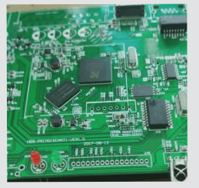
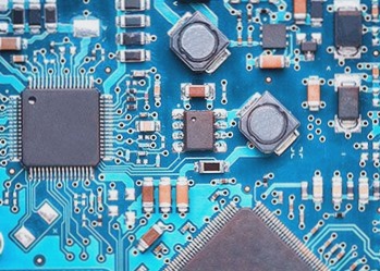
The Risks and Mitigation of EOS and ESD in PCBA
This article discusses the risks of Electrostatic Discharge (ESD) and Electrical Overload (EOS) in printed circuit board assemblies (PCBAs), highlighting the need for proper handling, design, and protection measures to prevent damage to sensitive components during assembly and testing.