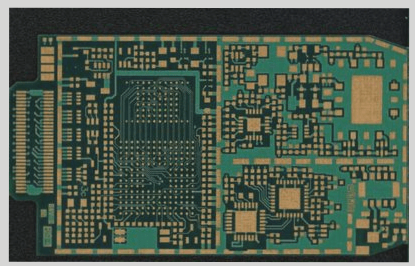
PCB reverse engineering focuses on key aspects such as component identification, layer structure analysis, and manufacturing process understanding.
In PCB reverse engineering, reconstructing the schematic involves dividing functional areas, identifying reference components, distinguishing different wire types, learning from similar designs, and reviewing the final schematic for accuracy and optimization to ensure it reflects the circuit’s operational principles.