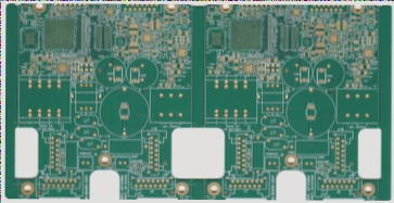
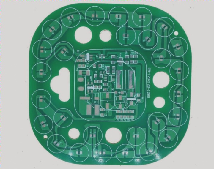
gbr file viewer

What is the process for self-inspection in PCB design?

This document outlines a comprehensive PCB design self-inspection process, covering structural design, component library, layout, routing, solder mask, silkscreen, vias, Gerber files, and PCB output files, with a focus on ensuring design accuracy, component alignment, and adherence to technical specifications.

What is the process for self-inspection in PCB design? Read More »

Understanding UL94 Ratings and Flame Retardant Materials in Injection Molding – WellCircuits

Introduction:UL 94 is a standard established by Underwriters Laboratories (UL) to evaluate the flammability of plastic materials used in devices and appliances. It provides a classification system bas…

Understanding UL94 Ratings and Flame Retardant Materials in Injection Molding – WellCircuits Read More »

Techniques for Testing PCB Circuit Boards

The five main PCB testing methods—manual visual inspection, automated optical inspection (AOI), functional testing, in-circuit testing (ICT), and X-ray inspection—each offer distinct advantages and limitations for ensuring the quality, reliability, and performance of circuit boards in electronic manufacturing.

Techniques for Testing PCB Circuit Boards Read More »

What are the key principles for anti-interference design in PCB?

The anti-interference design in modern PCB circuits is crucial for system performance and reliability, incorporating both hardware (e.g., noise suppression from power electronics) and software (e.g., digital filtering and redundancy) measures, along with detailed PCB layout principles like component placement, decoupling capacitors, power trace design, and grounding strategies to minimize noise and enhance stability.

What are the key principles for anti-interference design in PCB? Read More »

What are the methodologies for mixed-signal PCB design?

Contemporary mixed-signal PCB design faces challenges due to diverse digital logic devices, requiring systematic layout and wiring strategies to integrate distinct logic thresholds while isolating analog and digital noise for effective performance.

What are the methodologies for mixed-signal PCB design? Read More »

What is the design of a PCB stackup?

Multilayer PCB design requires that each trace layer has an adjacent reference layer and that power and ground layers are positioned closely to enhance coupling capacitance, while also focusing on minimizing loop areas of key signals to improve electromagnetic compatibility.

What is the design of a PCB stackup? Read More »

Advantages of PCB Performance and Application Scope

This text summarizes the characteristics and applications of hot-pressed silica gel products used in circuit boards, emphasizing their excellent heat conduction, fire resistance, and specific uses in the TFT-LCD assembly process, along with details on the weighbridge remote controller’s calibration and operational principles.

Advantages of PCB Performance and Application Scope Read More »

High-speed PCBs and soldered PCB assemblies

Engineers designing high-speed PCBs must prioritize optimal wiring and component placement to maintain signal integrity while minimizing layer count and spacing to reduce costs and crosstalk, following specific guidelines for lead length, differential signal management, and proper soldering practices to avoid defects.

High-speed PCBs and soldered PCB assemblies Read More »

Contact

WellCircuits
More than PCB

Upload your GerberFile(7z,rar,zip)