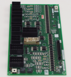
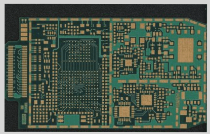
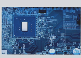
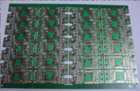
Which details are most beneficial for PCB engineers?
Attention to detail is crucial in PCB design, as the differences between novice and experienced engineers often lie in the careful consideration of component placement, spacing, and orientation to ensure successful manufacturing and performance.
Which details are most beneficial for PCB engineers? Read More »