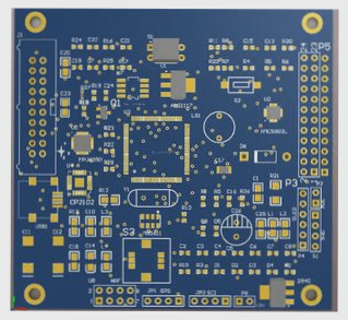
gerber viewer

Can you explain the principles of mixed-signal PCB layout design?

In designing high-density analog and digital circuits for a mixed-signal PCB, it’s crucial to achieve a balance between layout and routing while adhering to specific guidelines for signal integrity, bypass capacitor placement, and component proximity to minimize noise and optimize performance.

Can you explain the principles of mixed-signal PCB layout design? Read More »

What PCB layout and design skills do you possess?

In PCB design for connecting multiple devices, a star topology is generally preferred for signal integrity, but careful consideration of signal characteristics and wiring complexity is crucial, especially for high-speed signals, while the choice between automatic and manual wiring depends on software capabilities and efficiency, and ground connections must be separated for EMC and ESD considerations.

What PCB layout and design skills do you possess? Read More »

PCB Inspection Techniques and Risk Assessment

The text discusses various methods for testing PCB boards, highlighting the advantages and drawbacks of techniques such as visual inspection, electrical testing, automatic optical and X-ray inspections, laser detection, and size detection, while also addressing the hazards of improper handling during assembly.

PCB Inspection Techniques and Risk Assessment Read More »

The Unique Role of the PCB Immersion Gold Process

The immersion gold process is a costly surface treatment for circuit boards, essential for specific applications like gold fingers and fine line widths, but less suitable for others, and it offers advantages in heat dissipation, soldering strength, and measurement reliability compared to alternative methods like OSP and silver treatments.

The Unique Role of the PCB Immersion Gold Process Read More »

Considerations for Manufacturability in PCB Design

In electronic product manufacturing, prioritizing manufacturability in PCB design is crucial due to increasing assembly density and complexity, as inadequate designs can lead to costly modifications and delays, while effective component layout and assembly method selection significantly influence production efficiency and quality.

Considerations for Manufacturability in PCB Design Read More »

PCB Cleaning Procedures and Maintenance Protocols

The article discusses the importance of PCB boards in electronics, outlines cleaning procedures for residues after soldering, and introduces maintenance techniques to enhance reliability and solder joint integrity.

PCB Cleaning Procedures and Maintenance Protocols Read More »

Are you familiar with the principles of high-speed PCB design?

The article outlines essential principles for high-speed PCB layout design, emphasizing factors like signal quality, structural requirements, and thermal considerations, while detailing layout strategies, special component placement, and post-layout verification processes to ensure effective implementation.

Are you familiar with the principles of high-speed PCB design? Read More »

Methods for Removing Conformal Coating in PCBA Rework

The anti-paint protects electronic assemblies from environmental factors but must be carefully removed during repairs to avoid damaging components, and various methods exist for its removal, each suited to different types of coatings and application contexts.

Methods for Removing Conformal Coating in PCBA Rework Read More »

How does PCB circuit board design necessitate layout considerations?

The component arrangement on PCBs must meet electrical and mechanical requirements while adhering to SMT production standards, as effective layout design minimizes soldering defects and enhances overall performance.

How does PCB circuit board design necessitate layout considerations? Read More »

Ten Common Defects in PCB Design Process

The processing level definition is unclear, leading to potential mounting issues; excessive copper foil proximity to the outer frame risks warping; pads with filling blocks may pass design checks but fail in manufacturing; flower pad connections must avoid gaps; misaligned character pads complicate testing; short pads hinder probe alignment; single-sided pad apertures must be set correctly; overlapping pads can damage holes; excessive filling blocks complicate optical data; and misuse of graphic layers results in confusion, violating design standards.

Ten Common Defects in PCB Design Process Read More »

Contact

WellCircuits
More than PCB

Upload your GerberFile(7z,rar,zip)