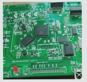
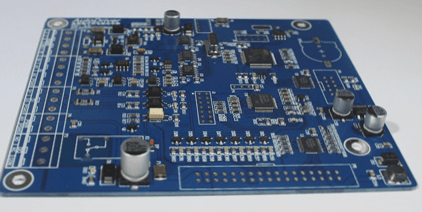
Are you familiar with designing PCBs to mitigate antistatic ESD?
Effective ESD protection in PCB board design involves strategic layering, proper layout, and meticulous installation. Adjustments during the design phase focus on adding or reducing components based on predictive analysis to mitigate ESD risks. Recommended preventive measures include utilizing multi-layer PCBs with dedicated ground and power planes, employing intertwined power and ground grids for double-sided PCBs, and implementing chassis ground traces below connectors vulnerable to ESD. These measures collectively enhance PCB resilience in diverse operational environments.
Are you familiar with designing PCBs to mitigate antistatic ESD? Read More »


