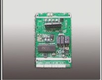
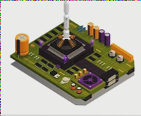
The PCB design should ensure distinct separation between AC and DC circuits, maintain a minimum distance of 5 mm between input and output terminals, clearly differentiate control and power circuits, avoid parallel high current and measurement lines, maximize copper usage, minimize long connections for high power, consider multi-layer boards for EMC, utilize large copper areas for interference-prone areas, avoid grounding loops, and organize high-power devices for effective cooling, while also focusing on appropriate grounding, wiring strategies to reduce crosstalk, and strategic decoupling capacitor placement to mitigate power supply noise.


