guidelines

Summary of Experience in Layout and Wiring of Mobile Phone RF PCBs

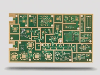
The revised text emphasizes that RF PCB design, often viewed as an arcane discipline due to its theoretical complexities, actually adheres to numerous practical guidelines crucial for achieving optimal performance and electromagnetic compatibility in mobile phones.

Summary of Experience in Layout and Wiring of Mobile Phone RF PCBs Read More »

Designing PCBs for High-power Applications

This article provides comprehensive guidelines for designing high-power PCBs, emphasizing the importance of precautions, trace width and thickness considerations, strategic PCB layout, component placement techniques, thermal management strategies, and material selection criteria.

Designing PCBs for High-power Applications Read More »

5 Common Flex PCB Design Issues

Flexible Printed Circuitry (FPC) offers extensive design flexibility over traditional PCBs but requires specialized considerations to ensure durability and manufacturability.

5 Common Flex PCB Design Issues Read More »

Minimizing Signal Coupling in RF Design

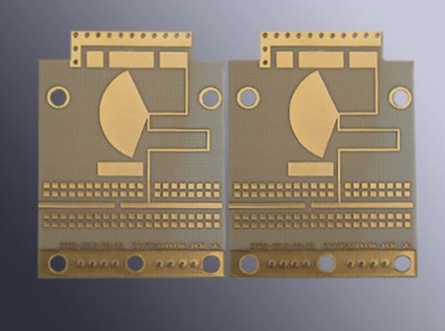
RF PCB board design is complex and challenging, with guidelines that must be carefully followed to accommodate various design constraints and overcome challenges such as integrating multiple functions in a compact space. Effective RF layout design involves isolating high-power and low-power circuits, implementing chip and power supply decoupling, and carefully placing components along the RF path to ensure signal integrity and minimize noise. Thorough planning and adherence to design principles are vital for successful RF layout design.

Minimizing Signal Coupling in RF Design Read More »

Key Points and Experience in USB 2.0 PCB Wiring

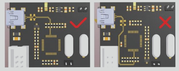
The USB is a fast, bidirectional, synchronous, inexpensive, and convenient hot-pluggable serial interface widely used for its advantages in data transfer speed, easy interface, and hot-swapping support. Proper PCB layout adhering to USB signal rules is crucial for stable operation of USB devices. Key points include keeping differential line length short, avoiding excessive vias, using symmetrical and parallel wiring, controlling line length mismatch within 5mil, maintaining distance from other signal networks, and ensuring proper line width and impedance for high-speed USB devices operating at 480 Mbits/s. Applying these guidelines will guarantee the reliable performance of USB devices.

Key Points and Experience in USB 2.0 PCB Wiring Read More »

Contact

WellCircuits
More than PCB

Upload your GerberFile(7z,rar,zip)