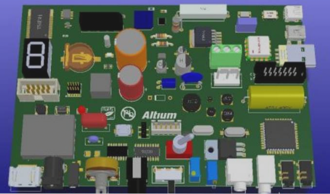
How do duplex PCBs utilize power and ground nets?
To prevent electrostatic discharge (ESD) damage in PCB designs, implement measures like multi-layer PCBs, tight signal and ground plane spacing, optimized routing, and effective grounding, while avoiding ESD-prone areas and using chassis grounding techniques.
How do duplex PCBs utilize power and ground nets? Read More »

