high-frequency grounding

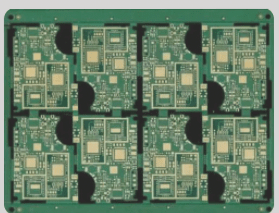
What are the key routing techniques for high-speed PCB design?

Key guidelines for designing high-frequency PCBs, including minimizing via layers, reducing lead lengths, avoiding signal trace bends, controlling crosstalk, isolating ground planes, and ensuring proper impedance matching to improve signal integrity and reduce noise, while also considering manufacturing complexity and cost.

What are the key routing techniques for high-speed PCB design? Read More »
Contact

WellCircuits
More than PCB

Upload your GerberFile(7z,rar,zip)