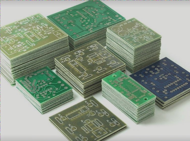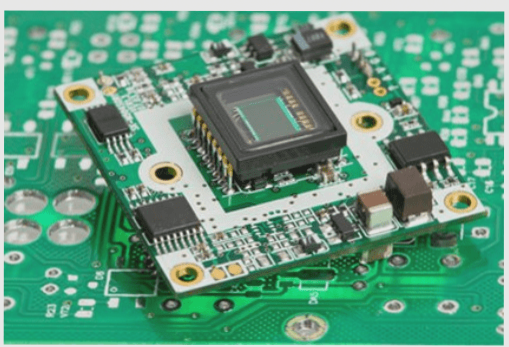
Key Considerations in High-Speed PCB Circuit Design
The PCB layout in high-speed circuit design is crucial for ensuring performance and manufacturability, with early planning, adherence to design principles, and attention to factors like signal integrity, component placement, and DFM guidelines helping to avoid costly redesigns and production delays.
Key Considerations in High-Speed PCB Circuit Design Read More »