high-speed PCB design.

Three Advanced Routing Techniques in PCB Board Design and Layout

The importance of PCB board design and wiring directly affects system performance, validated by high-speed design theories through layout, highlighting the critical role of wiring in high-speed PCB design. An analysis of encountered situations in actual wiring proposes optimized routing strategies focusing on right-angle, differential, and serpentine routing.

Three Advanced Routing Techniques in PCB Board Design and Layout Read More »

High-Speed PCB Board Design Using PROTEL

In high-speed PCB design using PROTEL software, adherence to specific layout and wiring principles is crucial to enhance reliability and effectiveness. These techniques not only shorten product development cycles but also boost market competitiveness through improved circuit performance and reduced errors.

High-Speed PCB Board Design Using PROTEL Read More »

Analyze high-speed PCB board design routing strategies

In high-speed PCB board design, differential signaling mitigates noise effects by transmitting signals as the difference between complementary pairs, ensuring effective noise reduction and supporting fast serial buses and double-data-rate memory extensively.

Analyze high-speed PCB board design routing strategies Read More »

Reasons for Using Multi-layer Circuit Boards in High-speed PCB Design: Enhanced Signal Integrity, Reduced Electromagnetic Interference.

Multi-layer circuit boards are essential for high-speed PCB design, providing benefits like enhanced power stability, reduced circuit impedance, and optimized wiring length, outweighing initial cost differences with single-layer alternatives.

Reasons for Using Multi-layer Circuit Boards in High-speed PCB Design: Enhanced Signal Integrity, Reduced Electromagnetic Interference. Read More »

Conventional PCB Drilling Techniques

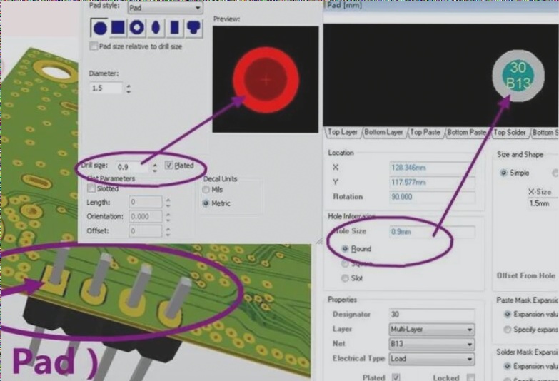
With the rapid development of the electronic industry, PCBs are evolving towards high density and precision, with different types of drilling holes emerging to meet production needs, such as through holes, blind holes, and buried holes. In high-speed PCB design, efforts can be made to reduce the adverse effects of parasitic effects caused by vias, such as choosing reasonable via hole sizes, using thinner PCB boards, minimizing unnecessary vias, and optimizing the placement of power and ground vias.

Conventional PCB Drilling Techniques Read More »

Contact

WellCircuits
More than PCB

Upload your GerberFile(7z,rar,zip)