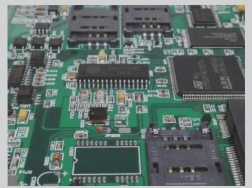
Design of High-Speed Signal Traces in PCBs
The article outlines key principles for high-speed PCB signal line routing, including the selection of appropriate layer counts, minimizing lead bends and lengths, reducing via usage, managing cross interference, implementing ground plane shielding, and proper grounding techniques for both digital and analog circuits to ensure signal integrity and reduce noise.

