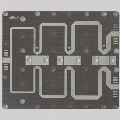
hot air leveling

The rationale for blocking the vias on the PCB board.

The evolving production process for printed circuit boards (PCBs) and the importance of via hole plugging to meet increasing demands in surface mount technology (SMT) and ball grid array (BGA) assemblies, detailing various methods for plugging via holes to prevent issues such as solder short circuits, flux residue, and false soldering during wave soldering, with a focus on maintaining technical accuracy and quality control throughout the process.

The rationale for blocking the vias on the PCB board. Read More »
Utilization of Peelable Adhesive Technology in PCB Manufacturing

This article examines peelable adhesives as a cost-effective alternative to special tapes for protecting gold plating and hot air leveling in PCB manufacturing, highlighting their advantages such as lower costs, ease of application, and no adhesive residue.

Utilization of Peelable Adhesive Technology in PCB Manufacturing Read More »

What are the various surface treatment processes for PCBs?

The document compares various PCB surface treatments, highlighting hot air leveling’s cost-effectiveness but environmental concerns, gold plating’s excellent conductivity at a higher cost, chemical gold’s complexity and potential reliability issues, electroless nickel palladium’s corrosion resistance with high palladium costs, and spray tin’s affordability with limited reliability for fine components.

What are the various surface treatment processes for PCBs? Read More »

Typical Applications of PCB Surface Treatment Processes

The choice of PCB surface treatment processes depends on the final assembly components, with five common methods including hot air leveling, organic coating, electroless nickel/immersion gold, immersion silver, and immersion tin, each offering specific advantages and limitations for different applications.

Typical Applications of PCB Surface Treatment Processes Read More »

How familiar are you with the PCB surface treatment process?

Although seemingly minor, current changes in PCB surface treatment processes are pivotal as environmental demands rise, driving future substantial evolution in ensuring excellent solderability and electrical properties.

How familiar are you with the PCB surface treatment process? Read More »

PCB Grounding and Surface Treatment Technologies”

As environmental concerns rise, PCB surface treatment processes, including hot air leveling, organic coating, and electroless nickel/immersion gold, are evolving to enhance solderability, electrical performance, and environmental impact.

PCB Grounding and Surface Treatment Technologies” Read More »

The PCB surface treatment process has been comprehensively summarized.

The processes described include various methods for PCB surface treatment: Hot Air Leveling, OSP, Nickel and Gold Plating, Gold Sink, Tin, Heavy Silver, Chemical Nickel Palladium, and Hard Gold Plating, each enhancing solderability, protection, or durability in different ways. Which specific aspect or process are you most interested in exploring?

The PCB surface treatment process has been comprehensively summarized. Read More »

6 Common PCB Surface Treatments

Common PCB surface treatment processes include lead-free or leaded tin spraying, hot air leveling (HAL), organic coating (OSP), chemical gold plating (electroless nickel/immersion gold), electroplating nickel gold, immersion silver, immersion tin, and halogen-free gold finger. Environmental concerns are driving a shift away from leaded processes towards lead-free options like tin spraying to comply with ROHS standards, crucial for passing audits and securing long-term product development partnerships. These treatments alter PCB components’ properties to ensure solderability and prevent oxidation, crucial for reliable electrical connections.

6 Common PCB Surface Treatments Read More »

Selecting PCB Surface Treatments: Expert Guide

The evolution of PCB surface treatment technology, influenced by environmental concerns and evolving industry standards, emphasizes lead-free and halogen-free processes like organic coating and electroless nickel plating/immersion gold, while also considering factors like component type and assembly requirements, leading to a dynamic landscape of options with a focus on meeting customer needs and environmental standards.

Selecting PCB Surface Treatments: Expert Guide Read More »

Contact

WellCircuits
More than PCB

Upload your GerberFile(7z,rar,zip)