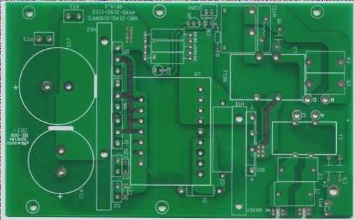
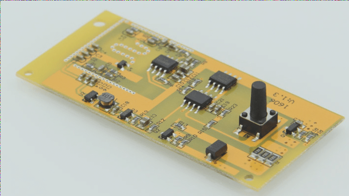
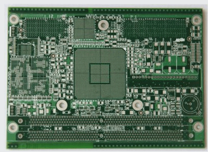
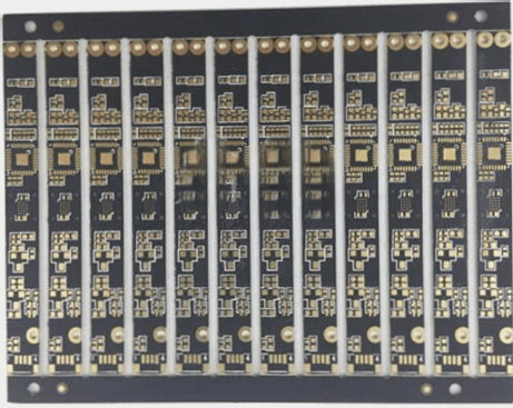
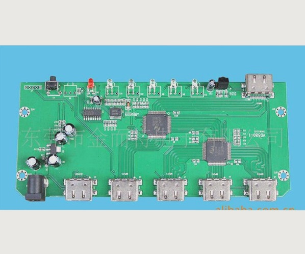
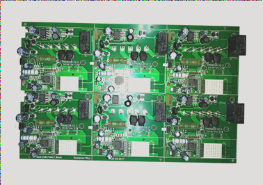
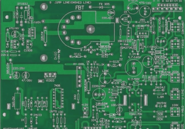
In the PCB manufacturing facility, the ‘repair line and PCB thickness’ are critical factors to consider.
In PCB manufacturing, wire patching is generally limited, especially on outer layers, with specific guidelines for repairs, such as one repair per board and adherence to IPC standards; edging is crucial to prevent contamination during various production stages, with trimming methods preferred for boards under 16 mil in thickness.

