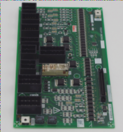
interference mitigation

How to design the PCB for a single-chip control board?

The circuit board design process involves three main steps: circuit schematic design, netlist generation, and PCB design, emphasizing careful component placement, decoupling capacitor positioning, and effective ground wire design to minimize interference and enhance reliability.

How to design the PCB for a single-chip control board? Read More »

PCB board design for the POWER circuit

Optimizing PCB layouts, particularly for the POWER circuit (DPS), demands meticulous attention to power plane dynamics and circuit characteristics, necessitating considerations like loop area minimization, trace width control, and strategic positioning to mitigate interference, especially for driving and sampling circuits.

PCB board design for the POWER circuit Read More »

Contact

WellCircuits
More than PCB

Upload your GerberFile(7z,rar,zip)