jlcpcb

Practical Guidelines for PCB Layout and Routing

High-integrity PCB design for high-speed circuits requires careful attention to layout, component placement, and power bypassing to ensure optimal performance and minimize interference, with detailed schematics and thorough review processes being crucial for success.

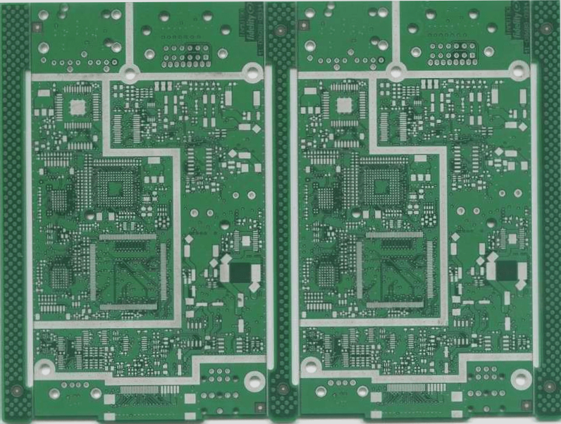
Practical Guidelines for PCB Layout and Routing Read More »

Features of the PCB Surface Mount Tool Board

Surface Mount Technology (SMT) offers advantages such as reduced size and weight, improved reliability, and higher production efficiency, enabling the use of advanced, miniaturized components in high-performance PCBs while supporting automation for cost-effective mass production.

Features of the PCB Surface Mount Tool Board Read More »

Techniques for Designing High Current Paths in PCB Layouts

To handle 100A of current on a PCB, several design strategies can be employed, including increasing copper thickness and trace width, using terminal blocks, incorporating custom copper busbars, and utilizing specialized manufacturing processes like 3-layer copper designs.

Techniques for Designing High Current Paths in PCB Layouts Read More »

Best Practices for PCB Circuit Board Design

PCB design requires meticulous attention to detail, thoughtful planning, and strategic rule-setting to ensure efficient, manufacturable, and high-performance designs, with an emphasis on anticipating user needs, organizing schematics, and optimizing layouts to minimize errors and reduce future revisions.

Best Practices for PCB Circuit Board Design Read More »

Design and Routing Process of Multi-Layer PCBs

PCB designers must follow key principles in multi-layer layouts and routing, including proper trace spacing based on electrical insulation, selecting appropriate cornering styles, determining trace width based on current and EMI considerations, and employing effective grounding and shielding techniques to minimize interference and enhance signal integrity.

Design and Routing Process of Multi-Layer PCBs Read More »

What are the different types of aluminum-based PCB substrates?

PCB aluminum substrates, also known as aluminum PCBs or MCPCBs, are superior to traditional FR-4 boards due to their exceptional heat dissipation, with flexible, hybrid, multilayer, and through-hole configurations offering advanced thermal management, cost efficiency, and design flexibility.

What are the different types of aluminum-based PCB substrates? Read More »

Ensure the PCB remains stable in the reflow oven to prevent any rocking.

To prevent PCB bending and warping during reflow furnace processing, minimize temperature impacts, use high Tg materials, increase board thickness, reduce board size, utilize furnace tray fixtures, and avoid V-Cut techniques.

Ensure the PCB remains stable in the reflow oven to prevent any rocking. Read More »

Contact

WellCircuits
More than PCB

Upload your GerberFile(7z,rar,zip)