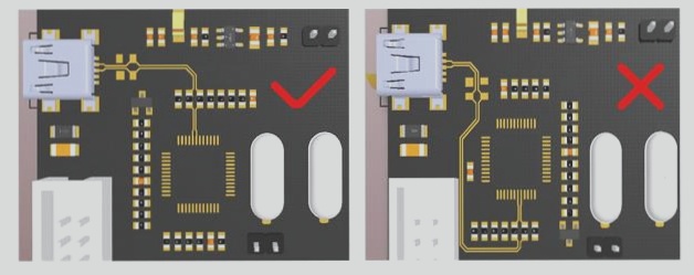
layout

4 Techniques for Multilayer PCB Identification

Printed Circuit Boards (PCBs) play a crucial role in electronic devices, serving as foundational infrastructure for connecting and transmitting electrical signals among electronic components. They are typically composed of materials like fiberglass and copper foil, offering excellent conductivity and mechanical properties. PCB design considerations include circuit connectivity, layout, and thermal management. Effective PCB layouts can minimize electromagnetic interference and signal delay, thereby enhancing overall device reliability and stability. Strict quality control and production processes are vital during PCB manufacturing to ensure high performance and extended product lifespan, ultimately influencing the overall quality and reliability of electronic devices.

4 Techniques for Multilayer PCB Identification Read More »

7 Techniques for Rapidly Assessing Circuit Board Design Quality: Part 2

This article introduces 7 ways to judge PCB design quality quickly, focusing on layout and component placement, warning new designers of common mistakes to avoid for a bad design. Review visible traces for straight segments without sharp bends, preferring standard green solder resist for easy inspection.

7 Techniques for Rapidly Assessing Circuit Board Design Quality: Part 2 Read More »

Basic design process and layout for PCB design.

The general PCB design process includes preliminary preparation, PCB structure design, PCB layout, wiring, wiring optimization, silk screen, network and DRC inspection, and plate making. Prior to starting the design, workers must sharpen their tools by preparing component libraries and schematics.

Basic design process and layout for PCB design. Read More »

Precautions for PCB Design – Part 2

Wiring is crucial in PCB design, impacting performance, electrical requirements, and aesthetics, following specific principles for optimal functionality and meeting requirements. Keep in mind priority of power and ground wires, position of high-demand lines, grounding for oscillators, wiring techniques, avoiding loops, and optimizing for production and maintenance testing. Pay attention to signal line and power line width, pad and via requirements, and pitch requirements for pads, lines, and vias.

Precautions for PCB Design – Part 2 Read More »

Summary of PCB Routing Techniques Experience

Layout is essential in PCB design, with wiring quality directly affecting system performance, especially in high-speed design where right-angle wiring should be avoided due to impedance discontinuity, and where differential routing offers advantages in immunity to interference and accurate timing positioning.

Summary of PCB Routing Techniques Experience Read More »

Ways to Prevent Electrostatic Discharge (ESD) in PCB Design

Effective anti-ESD design in PCB boards involves layering, proper layout, and installation, including precautions such as using multi-layer boards, placing signal layers close to power or ground layers, setting aside connectors, and connecting chassis ground and circuit ground.

Ways to Prevent Electrostatic Discharge (ESD) in PCB Design Read More »

PCB board design specifications for switching regulator production.

The PCB board is crucial in power supply design, with key considerations including electrical safety, component layout, high-frequency processing, global routing, and inspection for reliability.

PCB board design specifications for switching regulator production. Read More »

Key Points and Experience in USB 2.0 PCB Wiring

The USB is a fast, bidirectional, synchronous, inexpensive, and convenient hot-pluggable serial interface widely used for its advantages in data transfer speed, easy interface, and hot-swapping support. Proper PCB layout adhering to USB signal rules is crucial for stable operation of USB devices. Key points include keeping differential line length short, avoiding excessive vias, using symmetrical and parallel wiring, controlling line length mismatch within 5mil, maintaining distance from other signal networks, and ensuring proper line width and impedance for high-speed USB devices operating at 480 Mbits/s. Applying these guidelines will guarantee the reliable performance of USB devices.

Key Points and Experience in USB 2.0 PCB Wiring Read More »

High Frequency Printed Circuit Board Wiring Techniques

Protel software is widely used in China, but many designers only focus on its deployment rate without utilizing its improvements to adapt to changes in component characteristics, resulting in a waste of resources and hindering the performance of new devices. This article aims to introduce the general requirements for high-frequency circuit wiring and provide specific strategies for using Protel software for high-frequency circuit layout.

High Frequency Printed Circuit Board Wiring Techniques Read More »

Contact

WellCircuits
More than PCB

Upload your GerberFile(7z,rar,zip)