lithium phosphate vs lithium ion

KiCad – How to Design Differential Pair Traces – PCB Design Guide – Wellcircuits

AbstractHigh speed signals often use differential voltages to transfer the information between two points This technical solution is used either we are working in the analog or digital domain To tr

KiCad – How to Design Differential Pair Traces – PCB Design Guide – Wellcircuits Read More »

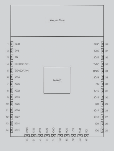
How to design a minimalist ESP32 breakout board – A comprehensive PCB design tutorial by Wellcircuits

The Rise of ESP32 in IoT Development ESP32 has emerged as a leading choice for microcontrollers in recent years, capturing the interest of IoT developers and hobbyists. Packed with a wide range of features like capacitive touch sensors, Hall sensors, and various interfaces, the ESP32-WROOM module has become a favorite among tech enthusiasts. Enhancing ESP32

How to design a minimalist ESP32 breakout board – A comprehensive PCB design tutorial by Wellcircuits Read More »

Overview of PCB (Printed Circuit Board) Design and Circuitry Explained

The process of PCB design involves simulation, component placement, efficient routing, adherence to manufacturing standards, EMC compliance, and final testing to ensure optimal functionality and minimize interference, all while balancing cost and performance.

Overview of PCB (Printed Circuit Board) Design and Circuitry Explained Read More »

PCB Simulation Design and Signal Integrity Analysis in PCB Systems

This article discusses the challenges and solutions in ensuring signal integrity and meeting timing requirements for DDR3 memory design in high-speed PCB systems, using Cadence’s time-domain analysis tool for simulation and offering design improvements to optimize system reliability.

PCB Simulation Design and Signal Integrity Analysis in PCB Systems Read More »

Electromagnetic Compatibility in the PCB Design Process

Electromagnetic compatibility (EMC) in PCB design is crucial for minimizing signal interference and improving system stability, achieved through careful layer configuration, signal routing, and grounding strategies to reduce noise and optimize performance.

Electromagnetic Compatibility in the PCB Design Process Read More »

Legend Printing in Multi-layer PCB Manufacturing Process – Step 12 – PCB Production Details – Wellcircuits

Legend printing also known as Silkscreen is a process of printing informational texts or patterns on the surface of the board Legend information includes component reference designators switch set

Legend Printing in Multi-layer PCB Manufacturing Process – Step 12 – PCB Production Details – Wellcircuits Read More »

GoWired Multiprotocol Gateway – Engineering Technical Specifications – Wellcircuits

GoWired Multiprotocol Gateway provides a powerful and excellent solution for wired automation systems It features a ARM M0 microcontroller with 8 times the ROM and the 16 times the RAM memory Two d

GoWired Multiprotocol Gateway – Engineering Technical Specifications – Wellcircuits Read More »

Automate the electronic design process for makers through comprehensive PCB design tutorials – Wellcircuits

Dear Wellcircuits CommunityAfter many years of suffering in PCB design we tried to do something to help makers design their own PCB prototypes quickly The resulting software is called EBE Electronic Bra

Automate the electronic design process for makers through comprehensive PCB design tutorials – Wellcircuits Read More »

Via-in-Pad Design: Key Considerations and Best Practices for PCB Manufacturing

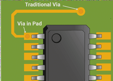
What is a Via-in-PadAs electronic products become increasingly miniaturized multi-functional and highly integrated PCBs need to accommodate higher routing densities To meet this demand via-in-pa

Via-in-Pad Design: Key Considerations and Best Practices for PCB Manufacturing Read More »

Contact

WellCircuits
More than PCB

Upload your GerberFile(7z,rar,zip)