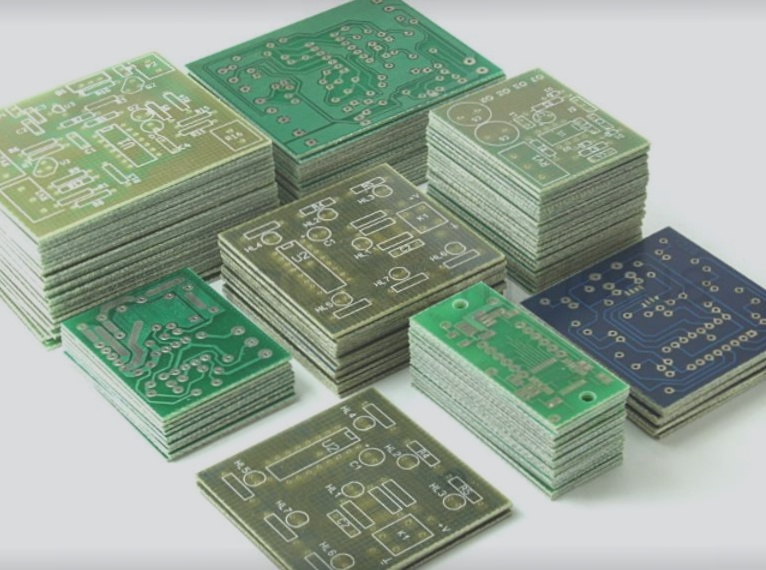
Considerations for PCB Board Stackup Design
When designing PCB board stack-up, pay attention to ensuring each trace layer has an adjacent reference layer and keeping the adjacent main power supply layer and ground layer apart to provide larger coupling capacitance. It’s important to consider the potential issues with different layer designs and their impact on EMI emissions and electromagnetic compatibility.

