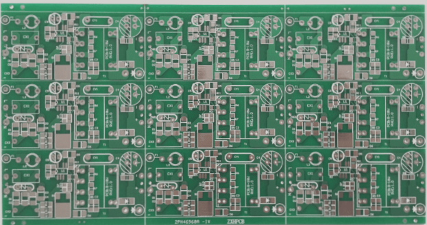
What do the various ‘layers’ in PCB manufacturing refer to?
The article outlines the various layers in PCB design using Protel 99SE, including signal layers for routing, internal plane layers for power and ground, mechanical layers for dimensions, solder and paste mask layers for solder application, keep-out layers for component placement, silkscreen layers for printed information, multilayer pads for connectivity, and drill layers for manufacturing specifications.
What do the various ‘layers’ in PCB manufacturing refer to? Read More »

