Multi-layer PCBs

Requirements for Supplying PCB Samples

PCB sample production is the initial manufacturing of printed circuit boards for testing and design validation before mass production, catering primarily to electronic engineers and researchers, and requiring specific parameters like material, layer description, and coating options.

Requirements for Supplying PCB Samples Read More »

Challenges with Power Distribution Networks in Multi-Layer PCBs

The article explores how EMI issues from power buses in multi-layer PCBs can be managed using techniques such as suppression coatings and proper layer design, focusing on enhancing IC performance and minimizing common-mode interference through appropriate power layer spacing and materials.

Challenges with Power Distribution Networks in Multi-Layer PCBs Read More »

Precision Coincidence Issue in Multilayer Blind/Buried Hole PCBs

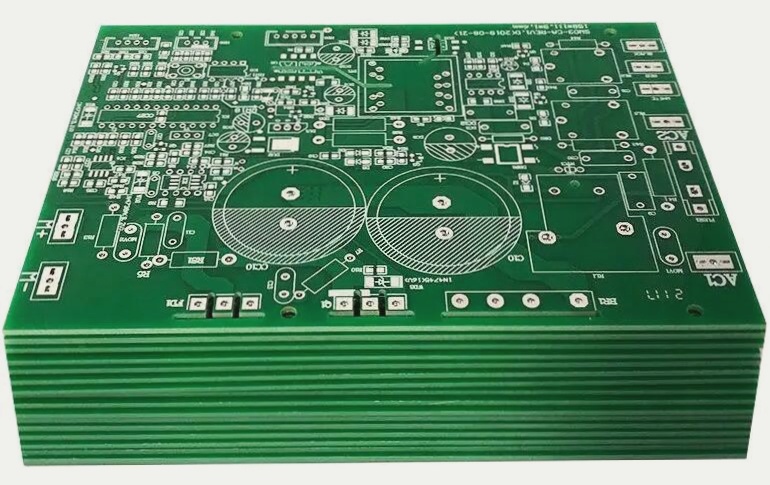
The key points can be summarized as follows: Multi-layer blind, buried, and blind-hole structure printed circuit boards (PCBs) are fabricated using the “sub-board” production method, which necessitates precise positioning due to multiple pressing, drilling, and hole plating processes. Buried, blind, and through-hole (multi-layer blind-buried circuit boards) combined technology is an important method for increasing the density of printed circuits. Buried and blind via holes are generally small in size and interconnected with the nearest inner layer, reducing the number of holes and simplifying the manufacturing process, thereby increasing the density of interconnections. The adoption of the pin front positioning system of ordinary multi-layer circuit board production unifies the graphic production of each layer, creating conditions for successful manufacturing of ultra-thick single chip PCBs.

Precision Coincidence Issue in Multilayer Blind/Buried Hole PCBs Read More »

Challenges in Prototyping Multilayer PCBs Production

Multi-layer PCB production faces challenges in inner circuit complexity, alignment between layers, pressing processes, and drilling production due to increasing requirements in various industries. Recommendations include designing wider line widths, ensuring even distribution of copper, and maintaining proper hole edge spacing.

Challenges in Prototyping Multilayer PCBs Production Read More »

Contact

WellCircuits
More than PCB

Upload your GerberFile(7z,rar,zip)