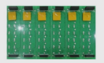
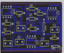
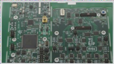
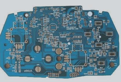
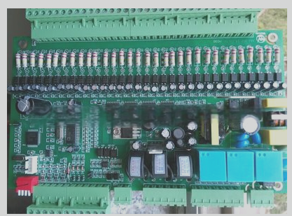
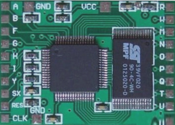
Benefits of Multi-Layer PCB Designs
Multilayer PCBs integrate multiple conductive layers in a compact design, offering advantages like increased circuit density, improved performance, enhanced reliability, and reduced weight, while also presenting challenges such as higher manufacturing costs, design complexity, and repair difficulties.