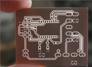
multilayer PCB structure

Design Methods for Multilayer Printed Circuit Boards

The design of a multilayer PCB requires careful consideration of electromagnetic compatibility (EMC) requirements, selection of appropriate layer count, and optimal stack-up structure to mitigate electromagnetic interference (EMI), ensuring effective signal routing, isolation, and power coupling.

Design Methods for Multilayer Printed Circuit Boards Read More »

PCB stackup design

General principles of layer arrangement for multilayer PCBs emphasize balancing wiring benefits against manufacturing complexity and cost. Designers prioritize symmetry and signal integrity, analyzing routing bottlenecks post component layout using EDA tools. They strategically place ground planes for shielding and reference, minimize crosstalk by avoiding adjacent signal layers, and optimize layer count based on signal type and interference requirements. For optimal PCB layering, considering the ultimate circuit performance remains paramount, ensuring effective signal isolation and minimal interference across various design scenarios.

PCB stackup design Read More »

Contact

WellCircuits
More than PCB

Upload your GerberFile(7z,rar,zip)