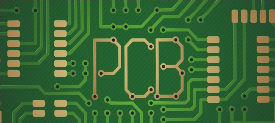
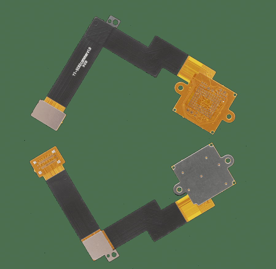
multilayer PCB

Fundamentals of PCB Board Lamination Process

The development of modern electronic science and technology increasingly demands higher precision in PCBs, with lamination playing a pivotal role in embedding copper layers within substrates to prevent unintended signal conduction or current flow. Various laminating processes cater to different PCB types, including multilayer and double-sided boards, as well as specialized laminates like PTFE for RF applications. PCB prototyping requires careful consideration of sample quantity, component assembly verification, and comprehensive electrical testing to ensure high-quality prototypes and smooth transition to mass production.

Fundamentals of PCB Board Lamination Process Read More »

Multilayer PCB: Advanced circuit board design.

A multilayer PCB, consisting of multiple layers of conductive traces separated by insulating layers, offers enhanced density, signal integrity, and thermal management, making it indispensable in various industries for complex electronic systems, evolving towards high-density, high-precision, and high-level digitalization.

Multilayer PCB: Advanced circuit board design. Read More »

The Impact of PCB Board Vias on Signal Transmission

Vias in multilayer PCBs play a crucial role, with drilling costs making up a significant portion of manufacturing costs. Parasitic capacitance and inductance of vias can impact signal quality and circuit speed, requiring careful consideration in high-speed PCB design. WellCircuits Limited offers a range of high-precision circuit boards to meet various customer needs.

The Impact of PCB Board Vias on Signal Transmission Read More »

Analysis of Common Problems in Circuit Boards

The thickness of the copper foil affects the thermal conductivity of the aluminum substrate, vias are used to connect electrical signals, soldering iron temperature is 200~300 degrees, unfilmed aluminum substrate can be easily scratched, LED lamp beads are soldered with a heating table, “is” on the circuit board is a stand-alone centrifugal switch mode, R+ is right channel positive output, L+ is left channel positive output, various processes for circuit boards, main switch board is generally a four-layer board, laminating process for multilayer pcb circuit boards involves prepreg bonding. WellCircuits Limited specializes in high-precision circuit board manufacturing.

Analysis of Common Problems in Circuit Boards Read More »

What is the maximum number of layers that a PCB can have?

Multilayer PCBs are designed with multiple conductive layers to achieve high-speed signal transmission and efficient processing, with factors affecting the number of layers including the purpose of the circuit board, signal type, through-hole selection, and signal layer and pin density. The main reasons for multilayer PCB design include improving signal integrity, space utilization, power layering, and thermal management, with advantages including reduced circuit impedance, improved energy transmission efficiency, and reduced equipment weight.

What is the maximum number of layers that a PCB can have? Read More »

Contact

WellCircuits
More than PCB

Upload your GerberFile(7z,rar,zip)