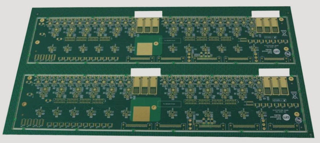
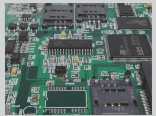
Certainly! Here’s a more professional revision of the phrase: “Industry-standard terminology frequently utilized in PCB (Printed Circuit Board) design.
This revised version enhances the clarity and structure of the article while maintaining its technical depth, providing insights into key PCB design concepts like annular rings, artwork films, basic grids, and blind via holes, as well as their roles in ensuring functional and reliable circuit designs.