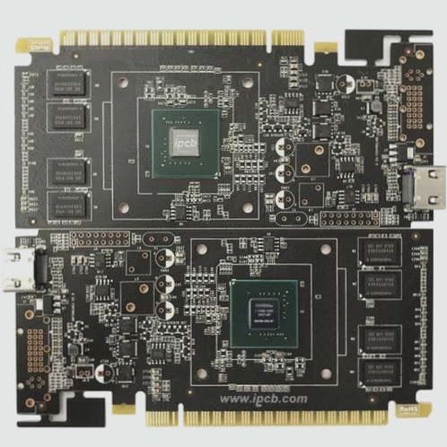
PCB Board

Conduct failure analysis on PCB failure cases.

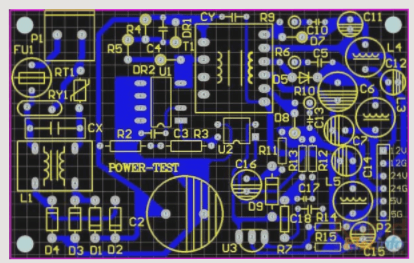
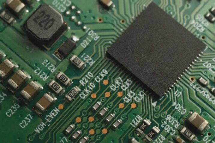
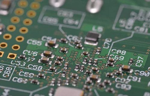
PCBs are critical components in electronic products, pivotal for signal transmission and housing various elements. Their quality directly impacts device performance. Evolving towards higher density and environmental sustainability presents challenges like production failures, necessitating rigorous failure analysis to identify causes, propose solutions, and ensure accountability.

Conduct failure analysis on PCB failure cases. Read More »

Traditional PCB Temperature Profile of System Components

A classic PCB board temperature profiling system includes a data collection profiler traversing the furnace center to gather PCB temperature data via affixed Type K thermocouples. Insulation shields the thermocouples from furnace heat, with software analyzing data to assess soldering outcomes and detect adverse trends, crucial for maintaining final PCB product quality.

Traditional PCB Temperature Profile of System Components Read More »

Guide to Wave Soldering Avoidance

Tin appearance on PCB boards post-wave soldering may arise from various factors beyond just design flaws. Issues like inadequate flux activity, uneven application, or uncontrolled solder temperature can contribute. While not all issues stem from design, designers must ensure correctness. To mitigate tin formation, focus on flux activity, wettability, and solder temperature during wave soldering.

Guide to Wave Soldering Avoidance Read More »

Analysis of Synchronous Switching Noise Generated by FPGA on PCB

Today’s CMOS technology allows a single FPGA device to have multiple I/O interfaces, and it is crucial for FPGA users to accurately measure and quantify system-level SSN on the PCB board. This article provides a comprehensive introduction to SSN, with a specific focus on SSN caused by FPGA output buffering, and presents several PCB board design techniques that can effectively reduce SSO.

Analysis of Synchronous Switching Noise Generated by FPGA on PCB Read More »

Specifications for non-electrolytic nickel plating on PCBs

The statement can be summarized as follows: “Non-electrolytic nickel coating on PCB boards serves multiple functions, including facilitating gold deposition, establishing strong connections, and preventing solder issues due to oxides or contaminants. Nickel’s purity is crucial for gold precipitation, with a balance of phosphorus content ensuring desired properties. Hardness matters for physical strength, especially in automotive applications. Copper is preferred for circuits, while gold’s conductivity is valuable for outer layers. Nickel’s thickness can impact high-frequency signals, and contact resistance is vital for long-term conductivity.”

Specifications for non-electrolytic nickel plating on PCBs Read More »

What are the essential parameters that manufacturers require for PCB prototyping?

Before PCB mass production, customers need to provide detailed parameters for prototype creation, which helps assess manufacturer capabilities, minimize defects, and establish a foundation for future production. This includes sheet selection guidelines, thickness descriptions, copper skin thickness, solder mask color specifications, special production requirements, dimensional tolerances, sample quantities, and imposition requirements.

What are the essential parameters that manufacturers require for PCB prototyping? Read More »

Contact

WellCircuits
More than PCB

Upload your GerberFile(7z,rar,zip)