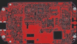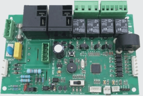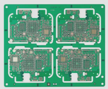
Thermohygrometer for SMT Soldering Process Monitoring
During SMT patch processing, factories must install suitable temperature and humidity meters, maintain specific environmental conditions, ensure cleanliness, and meet air source, exhaust, and lighting requirements.
Thermohygrometer for SMT Soldering Process Monitoring Read More »