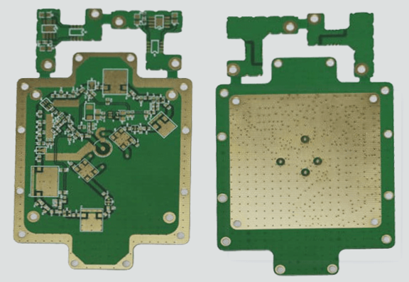
PCB component layout

The specifics of the PCB schematic reverse engineering process.

PCB copy board (or reverse engineering) involves analyzing a physical circuit board to recreate its design files, schematic diagrams, and other technical documents, which are then used to replicate the original PCB.

The specifics of the PCB schematic reverse engineering process. Read More »

What PCB materials are required for fabricating a PCB clone?

PCB board selection involves choosing materials like copper laminates based on factors like electrical performance, reliability, and cost, with different laminates offering specific advantages for different applications, such as flame-retardant boards or those optimized for high frequencies.

What PCB materials are required for fabricating a PCB clone? Read More »

Comprehend the design principles of PCBA boards

The PCB design process involves three main steps: schematic design, netlist generation, and PCB layout. Specific requirements include optimizing component placement and trace routing to minimize interference, such as separating parallel signal lines with a ground wire and aligning adjacent layer traces perpendicularly. Effective grounding involves placing separate power and ground planes perpendicular across layers. Trace widths are critical, with wider ground traces recommended for digital circuit PCBs to establish a robust ground network.

Comprehend the design principles of PCBA boards Read More »

Contact

WellCircuits
More than PCB

Upload your GerberFile(7z,rar,zip)