PCB components

Why are PCBs Green? – Flexible PCB – Wellcircuits

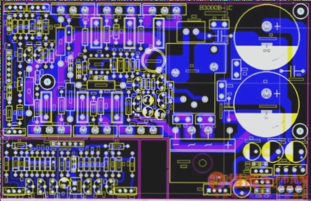
回路基板の構造回路基板は主にパッドオーバーホール取り付け穴ワイヤ部品コネクタパディング電気境界などで構成されている各コンポーネントの主な機能は以下の通りですパッド部品のピンを溶接するための金属穴貫通金属貫通と非金属貫通があり金属貫通は層間素子ピンを接続するために使用される取り付け穴回路基板を固定するワイヤ部品ピンの電気ネットワークを接続するための銅フィルムコ

Why are PCBs Green? – Flexible PCB – Wellcircuits Read More »

Analysis of Surface-Mount Technology (SMT) in Electronics

Surface Mount Technology (SMT) has revolutionized electronic assembly by replacing traditional through-hole methods, improving product reliability, reducing costs, and enhancing both consumer and military electronics through processes like printing, placement, and reflow soldering.

Analysis of Surface-Mount Technology (SMT) in Electronics Read More »

Professional expertise in PCB (Printed Circuit Board) design and technology.

A PCB (Printed Circuit Board) serves as the foundation for electronic devices, providing both mechanical support and electrical connections between components, with variations like single-sided, double-sided, and multi-layer designs to accommodate different complexities in circuitry.

Professional expertise in PCB (Printed Circuit Board) design and technology. Read More »

The composition of PCB design for circuit boards.

The current PCB circuit board consists of key components including circuits, dielectric layers, holes, solder masks, silk screens, and surface finishes, which collectively enhance its density, reliability, designability, manufacturability, testability, assemblability, and maintainability.

The composition of PCB design for circuit boards. Read More »

Key Components and Primary Functions of PCB Design

Comprehensive overview of printed circuit boards (PCBs), detailing their components, manufacturing processes for single-layer, double-layer, and multi-layer structures, and the functions of various layers within the PCBs.

Key Components and Primary Functions of PCB Design Read More »

Which components are present on the printed circuit board (PCB)?

The PCB comprises various components and processing technologies, featuring single-layer, double-layer, or multi-layer structures, each with distinct production methods and functional layers, including signal, protective, silk screen, and internal layers.

Which components are present on the printed circuit board (PCB)? Read More »

PCB Component Selection, Testing Procedures, and Quotation Methods

A mobile phone’s small battery involves selecting PCB components based on criteria like protection ICs, MOSFETs, capacitors, resistors, and other elements, with detailed considerations for design, electrical performance, and quotation methods.

PCB Component Selection, Testing Procedures, and Quotation Methods Read More »

Defects in Reflow Soldering and BGA Package Circuits

Emergency methods for addressing BGA integrated circuit soldering issues include using solder paste to enhance solder ball adhesion, employing a hot air gun to heat the chip evenly, and applying moderate pressure to ensure proper contact between the solder balls and the PCB. These methods are crucial for effective repair under non-professional conditions.

Defects in Reflow Soldering and BGA Package Circuits Read More »

Regarding the transition from PCB schematic to layout

Key steps in transferring PCB schematics to layout include grid setup, defining blank areas and vias, adjusting pad/via parameters, establishing design rules, customizing shortcut keys, managing schematic errors, synchronizing design updates with annotation, renumbering devices, and handling last-minute changes effectively.

Regarding the transition from PCB schematic to layout Read More »

Contact

WellCircuits
More than PCB

Upload your GerberFile(7z,rar,zip)