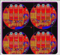
Comprehension of fundamental concepts in PCB design
The key to reducing EMI in PCB design involves stack arrangement to minimize signal return path length, reduce coupling, and mitigate interference, while copper pours are crucial for EMC, PCB processing, signal integrity, and thermal management, and signal routing considerations must prioritize signal speed, timing, and integrity, particularly in systems with DSPs and PLDs.
Comprehension of fundamental concepts in PCB design Read More »

