PCB design guidelines

What are the fundamental guidelines for PCB circuit routing?

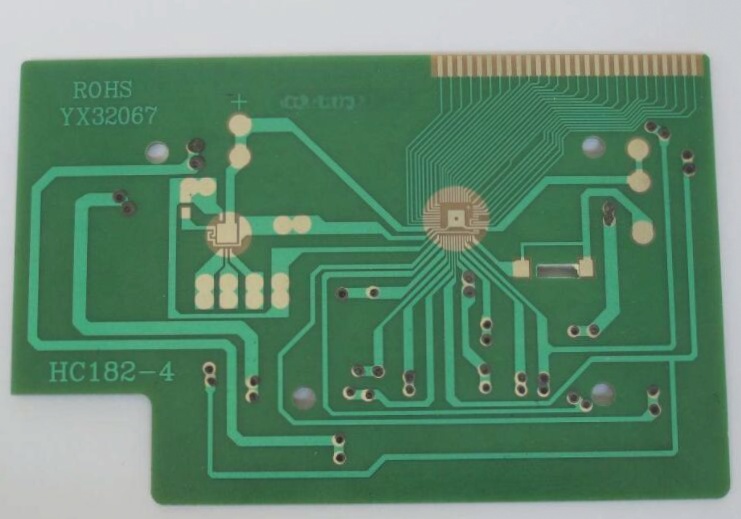
This document outlines PCB design rules, including trace width and spacing requirements, grounding guidelines, crosstalk control, routing direction, impedance matching, trace length management, and resonance prevention to ensure signal integrity, minimize interference, and optimize performance.

What are the fundamental guidelines for PCB circuit routing? Read More »

PCB design layout and component orientation

PCB design should prioritize structured layout, optimal trace width and spacing, minimal trace bends, accurate component pin sequencing, proper component placement, and careful consideration of input/output terminal positioning, while ensuring efficient wiring, easy maintenance, and alignment with the schematic.

PCB design layout and component orientation Read More »

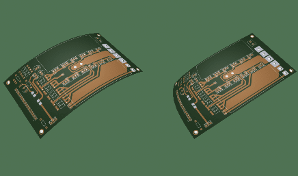
What are PCB Bow and Twist? An Overview of PCB Deformation – Basic PCB Knowledge from Wellcircuits.

Ideally PCBs should be perfectly flat however this is not always possible Bow and twist usually occur PCB bow and twist are two common types of board warpage that can occur during and after the P

What are PCB Bow and Twist? An Overview of PCB Deformation – Basic PCB Knowledge from Wellcircuits. Read More »

Address the challenges associated with aligning multiple connector arrays across PCB boards.

PCB manufacturers face significant challenges in miniaturizing connectors, managing tight tolerances, and maintaining alignment between multiple connectors on dense PCBs, requiring clear guidelines and collaboration with suppliers to ensure performance, reliability, and cost-effectiveness.

Address the challenges associated with aligning multiple connector arrays across PCB boards. Read More »

Temperature shock testing of PCB circuit boards in manufacturing facilities.

To minimize crosstalk on PCB circuit boards, avoid long parallel traces, increase spacing between lines, and reduce signal line crossings, while grounding sensitive signal lines effectively mitigates interference.

Temperature shock testing of PCB circuit boards in manufacturing facilities. Read More »

PCB Design for S-Touch™ Capacitive Touch Controller

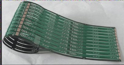
This application note provides PCB layout guidelines for S-TouchTM capacitive touch sensing using common FR4 and flexible PCBs, focusing on optimizing two-layer PCB designs with specific recommendations for sensor electrode placement, signal trace routing, and grounding to enhance sensitivity and minimize noise interference.

PCB Design for S-Touch™ Capacitive Touch Controller Read More »

Fundamentals of Component Orientation in PCB Design

In PCB design, follow a systematic layout order, ensure proper trace width and spacing, simplify routing, maintain correct pin arrangement and component spacing, align with the schematic diagram, and design for efficient wiring with neat and aesthetically pleasing placement of components.

Fundamentals of Component Orientation in PCB Design Read More »

Contact

WellCircuits
More than PCB

Upload your GerberFile(7z,rar,zip)