PCB factories

Common knowledge in PCB factories shared

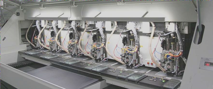
PCB manufacturing commonly faces various defects due to factors such as machine errors or human mistakes, including issues like “hole breakout” and “point PCB breakout.” These defects arise from inadequate slag removal processes during PCB processing, affecting product quality.

Common knowledge in PCB factories shared Read More »

Blind and Buried Via PCB fabrication services within a High Density Interconnect (HDI) PCB processing environment.

Modern electronic devices require PCB factories to adopt multi-layer HDI PCB buried blind via processing solutions to accommodate the large number of components on the surface, necessitating fine conductor widths and narrower spacing between them. WellCircuits Limited specializes in producing high-precision double-sided, multi-layer, impedance-controlled, blind buried vias, and thick copper circuit boards to meet customer demands for various products.

Blind and Buried Via PCB fabrication services within a High Density Interconnect (HDI) PCB processing environment. Read More »

Three Primary Causes of Copper Rejection in PCB Manufacturing Facilities

The main reasons for copper rejection in PCB factories are over-etched copper foil, local collisions during manufacturing, and unreasonable PCB circuit design, leading to insufficient bonding strength and eventual copper wire detachment.

Three Primary Causes of Copper Rejection in PCB Manufacturing Facilities Read More »

Contact

WellCircuits
More than PCB

Upload your GerberFile(7z,rar,zip)