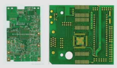
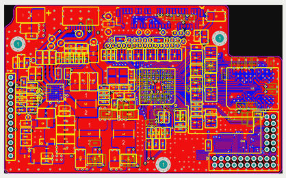
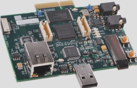
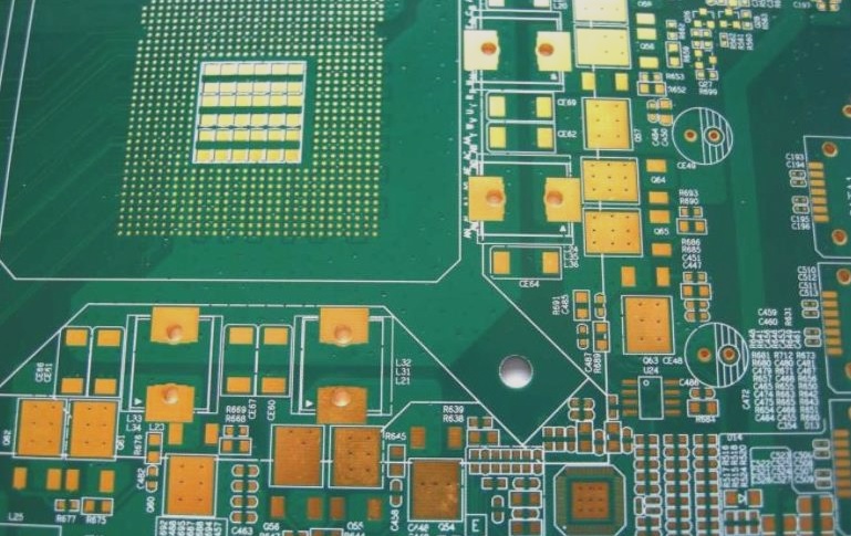
PCB INSPECTION

What are the various inspection technologies used for PCB boards?

The advent of surface mount technology has led to the need for cost-effective automatic inspection of PCB multilayer boards, with common testing methods including the bed of needles and flying probe tests, each with their own advantages and limitations depending on board complexity, testing speed, and cost considerations.

What are the various inspection technologies used for PCB boards? Read More »

Methods for Detection of Multilayer PCB Assemblies and SMT Processes

The article discusses various inspection methods for ensuring the quality and reliability of assembled PCB multilayer circuit boards, including the use of Automatic Optical Inspection (AOI), X-ray, ultrasound, laser, and infrared detection systems, as well as manual visual inspections, with a focus on key stages in the SMT process such as solder paste printing, component placement, and soldering.

Methods for Detection of Multilayer PCB Assemblies and SMT Processes Read More »

Technology-Driven Approach to PCBA Quality Control

PCBs are essential to all electronic devices, and as their design capabilities advance, rigorous quality assurance testing becomes crucial to ensure high-quality production, minimize defects, and avoid disruptions in manufacturing and supply chains.

Technology-Driven Approach to PCBA Quality Control Read More »

Methods for Directly Determining the Number of PCB Layers

Various methods, including visual inspection, via hole analysis, and industry insights, can be used to estimate the number of layers in a PCB, though each has limitations in terms of accuracy and reliability.

Methods for Directly Determining the Number of PCB Layers Read More »

Emphasize the evaluation of the PCB design workflow.

After finalizing a PCB layout and routing, a critical yet often overlooked step is post-inspection, which is essential to prevent issues like insufficient trace width and improper component placement that could lead to costly manufacturing problems.

Emphasize the evaluation of the PCB design workflow. Read More »

PCB Component Placement and Clearance Analysis

After PCB design, essential inspections include verifying manufacturing requirements, component alignment, 3D graphics, production line optimization, work instructions, inspection rules, and software compatibility to ensure quality and functionality.

PCB Component Placement and Clearance Analysis Read More »

PCB design for manufacturability and fabrication processes.

Once PCB design is complete, a comprehensive inspection is crucial, including DFM review, component alignment verification, 3D modeling, production line optimization, and other detailed checks to ensure the design meets all functional and manufacturing requirements.

PCB design for manufacturability and fabrication processes. Read More »

The Most Comprehensive PCB Circuit Design Inspection Criteria

After completing the PCB design, thorough inspection is crucial to ensure design integrity across all aspects, including electrical characteristics, physical attributes, mechanical factors, and installation requirements.

The Most Comprehensive PCB Circuit Design Inspection Criteria Read More »

Contact

WellCircuits
More than PCB

Upload your GerberFile(7z,rar,zip)