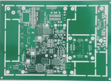
What is the design of a PCB stackup?
Multilayer PCB design requires that each trace layer has an adjacent reference layer and that power and ground layers are positioned closely to enhance coupling capacitance, while also focusing on minimizing loop areas of key signals to improve electromagnetic compatibility.