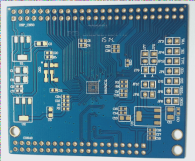
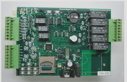
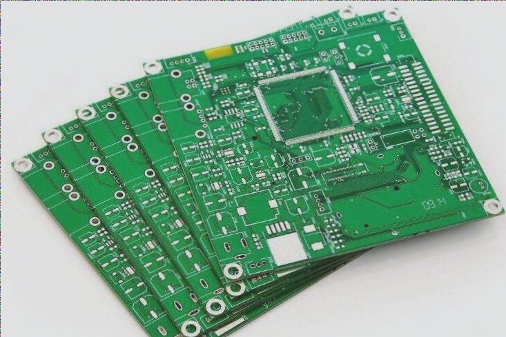
PCB layers

Rigid and Flexible PCB Circuit Board Wiring

PCBs (Printed Circuit Boards) come in rigid, flexible, and rigid-flex types, with variations in thickness, materials, and layers (single-sided, double-sided, or multilayer), offering advantages like high density, reliability, design flexibility, and manufacturability for use in complex electronic systems.

Rigid and Flexible PCB Circuit Board Wiring Read More »

Fundamentals of PCB Design and Circuit Board Engineering

The “layers” in PCB design refer to the actual physical copper layers of a circuit board, with modern designs often including multiple layers for routing and power distribution, while concepts like vias, silk screen, SMD components, and fill areas must be carefully managed to ensure a functional and manufacturable design.

Fundamentals of PCB Design and Circuit Board Engineering Read More »

PCB manufacturing cost and board flexibility (bending tolerance)

The choice between even and odd-layer PCBs depends on factors like cost, manufacturing complexity, and risk of bending, with odd-layer designs potentially reducing material costs but increasing processing difficulty and risk of warping.

PCB manufacturing cost and board flexibility (bending tolerance) Read More »

The various layers in PCB design

The various layers in PCB design, including mechanical, routing, silkscreen, solder mask, and drilling layers, as well as how to configure a 4-layer PCB in PowerPCB, highlighting design considerations such as signal integrity, routing strategies, and the selection of PCB software for optimal results.

The various layers in PCB design Read More »

What do the various ‘layers’ in PCB manufacturing refer to?

The article outlines the various layers in PCB design using Protel 99SE, including signal layers for routing, internal plane layers for power and ground, mechanical layers for dimensions, solder and paste mask layers for solder application, keep-out layers for component placement, silkscreen layers for printed information, multilayer pads for connectivity, and drill layers for manufacturing specifications.

What do the various ‘layers’ in PCB manufacturing refer to? Read More »

Electronic components and printed circuit boards

Printed circuit boards (PCBs) are essential for connecting electronic components, with their development and design focused on reducing wiring errors, improving efficiency, and evolving in complexity and precision, with China currently leading in global production and innovation.

Electronic components and printed circuit boards Read More »

How can one ascertain the number of layers required for a PCB design?

To determine the number of layers in a PCB, observe the via holes and light transmission: if vias are visible on both sides, it’s likely a 4-layer board; if vias are visible only on one side or light passes through them, it could be a 6/8-layer board; multilayer boards with opaque inner cores may have many more layers.

How can one ascertain the number of layers required for a PCB design? Read More »

Explanation of the analytical procedures for PCB prototyping parameters.

PCB proofing involves sending a PCB layout design to a manufacturer for trial production, with key considerations including material type, board layers, solder mask and silkscreen colors, copper thickness, via coverage, surface coating, and quantity.

Explanation of the analytical procedures for PCB prototyping parameters. Read More »

An Overview of Differences in Multilayer Circuit Boards

PCBs, initially used in radios in the 1930s and 1940s, have evolved from direct wiring to complex multilayered boards with various signal, power, silkscreen, mechanical, and masking layers, crucial for modern electronics design and manufacturing.

An Overview of Differences in Multilayer Circuit Boards Read More »

Contact

WellCircuits
More than PCB

Upload your GerberFile(7z,rar,zip)